
Cheng Feng 20 years focus on plasma cleaning
technology research and development
National High-tech Enterprise
National consulting hotline:
Free proofing is available for consultation by appointment
Popular Articles
Contact Us
Service Hotline
13632675935
CRF
Address: 1303, Building 3, Manjinghua Science and Innovation Workshop, No.6 Songjiang Road, Songgang Street, Bao'an District, Shenzhen, China.
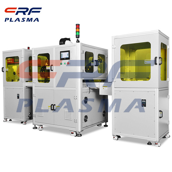
Etching of metal hard mask layer in large plasma cleaning machine
Keywords:
Published on:
15 Dec,2020
Etching of metal hard mask layer in large plasma cleaning machine:
Using metal as large plasma cleaning machine groove process in the first groove etching hard mask layer can significantly reduce (ultra) low dielectric constant material damage, improve the metal wires twisted and roughness and control structure of double Damascus zhongtong between holes and grooves flat smooth transition transformation, from 45 nm technology node begins to be after a period of consolidation is widely used.
Since the metal hard mask pattern etched by large plasma cleaner will be used as the mask layer for groove etching, the graphic integrity and key size of the metal hard mask layer etched will be transferred to (super) low dielectric constant material again, and the metal wire will be formed after groove etching. Metal hard mask layer after etching graphic design graphics for the transmission of fidelity, etching after the key size deviation of load effect, will be the subsequent etching grooves inheritance or even due to the load effect of etching grooves will continue to enlarge the deviation, as a result, large plasma cleaning machine need to strictly control the metal etching hard mask layer. The smaller the load effect is, the higher the fidelity of the designed metal line graph is. The graphics can be transferred strictly from the mask through exposure and development to the metal hard mask layer, and the lateral wall contour Angle of the metal hard mask is approximately vertical, which is the requirement of the process integration for the metal hard mask layer etching process.
Typical large plasma cleaning machine metal hard mask etching process is generally photoresist and bottom anti-reflective layer organic material as a single etching mask structure.
Hot Products
Related articles

CRF
National Service Hotline
Contact Email
Address:1303, Building 3, Manjinghua Science and Innovation Workshop, No.6 Songjiang Road, Songgang Street, Bao'an District, Shenzhen, China.
Add WeChat
Get related information
Links

Cheng Feng Zhi Zuang a focus on plasma research and development for 20 years
We
The services of
Inquire for free sample testing
1-to-1 program customization
24-hour online after-sales service
Source manufacturer

Scan the code for information
