
Cheng Feng 20 years focus on plasma cleaning
technology research and development
National High-tech Enterprise
National consulting hotline:
Free proofing is available for consultation by appointment
Popular Articles
Contact Us
Service Hotline
13632675935
CRF
Address: 1302, Building 3, Manjinghua Science and Innovation Workshop, No.6 Songjiang Road, Songgang Street, Bao'an District, Shenzhen, China.
IC semiconductor field
Keywords:
Published on:
28 Jul,2020
1、COB/COF/COG
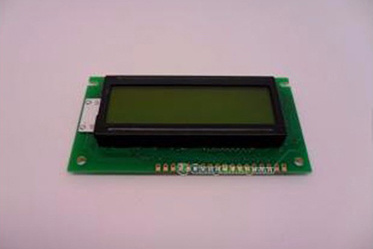
With the rapid development of smart phones, people's requirements for cell phone camera pixels are getting higher and higher, and nowadays the pixels of cell phone camera modules made by traditional CSP packaging process can no longer meet people's needs, and cell phone camera modules made by COB/COG/COF packaging process have been used in a large number of megapixel cell phones, but their manufacturing yields are often only about 85% due to their process characteristics. 85% or so, and the cause of the cell phone yield is not high mainly because of the centrifugal cleaning machine and ultrasonic cleaning can not do high cleanliness cleaning holder and Pad surface pollutants, resulting in holder and IR adhesion is not high and bonding bad problems, by plasma cleaning machine equipment to remove the holder on the organic pollutants and activation of the substrate, so that its adhesion with Plasma etching machine plasma surface treatment machine can also remove the oxide on the surface of the pad and roughen the surface, significantly improve the success rate of banding once.
2、Semiconductor silicon wafers ( Wafer )
IC chip manufacturing field, plasma cleaning machine equipment plasma processing technology has been an irreplaceable mature process, plasma etching machine whether in the chip source ion injection, or wafer coating, or our low-temperature plasma surface treatment equipment can achieve: in the wafer surface to remove oxide film, organic matter, to mask and other purification treatment and surface activation to improve the wafer surface wettability.

Hot Products
Related articles

CRF
National Service Hotline
Contact Email
Address:1303, Building 3, Manjinghua Science and Innovation Workshop, No.6 Songjiang Road, Songgang Street, Bao'an District, Shenzhen, China.
Add WeChat
Get related information
Links

Cheng Feng Zhi Zuang a focus on plasma research and development for 20 years
We
The services of
Inquire for free sample testing
1-to-1 program customization
24-hour online after-sales service
Source manufacturer

Scan the code for information
